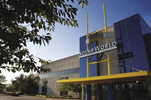
The SolarWorld manufacturing plant in Hillsboro, Ore., fronts the city’s Deer Park Industrial Park on a 97-acre property. Inside, 1,000 employees work four shifts 24/7 producing crystalline silicon photovoltaic (PV) panels.
As you approach, the plant’s white façade sits back from the road about 400 feet, and you notice the company promotes solar power even in its parking lot, where the visitor’s carport is topped by solar panels.
Entering the building, there’s a map of the world in the lobby that chronicles the company’s global reach with tiny dots over cities where SolarWorld has offices: Hillsboro, Ore.; Freiberg, Germany; Singapore; and Cape Town, South Africa.
Then Ben Santarris, head of corporate communications and sustainability for the Americas, walks into the lobby, shakes your hand and asks if you are ready for the tour.
“We do all four steps in this plant,” Santarris says. “We’re the only large company in the country that does that. We’re a pure-play solar company, and we will continue to be such. We are all solar, all the time.”
The Meltdown
Santarris’ first stop is a hallway. He pauses for a moment before speaking. Then he helps you understand why the hallway is important.
“This hallway separates our first and second steps of the process,” Santarris says. “We designed the factory this way so that the people working on the first step and the people working on the second step have to interact regularly.
“No one here works in isolation,” he continues, walking down the hallway toward a room that looks more hospital operating room than factory floor. “Everyone is dependent on everyone else, so we designed our factory to encourage collaboration.”
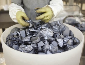
Santarris pushes open the swinging door to a room filled with workers clad in facemasks and hospital scrubs. They are hovering over giant pots and are putting what appear to be rocks in them. Santarris nods when you ask what they are doing.
“Those are pieces of polysilicon that they are putting in the crucibles,” Santarris says, putting a name to the pots. “Everything starts with those chunks. We also put in pieces of silicon that are recycled from later in the process — but I don’t want to get ahead of myself.”
Each crucible holds 250 lb of polysilicon chunks stacked on top of each other — and one additional silicon disk infused with a boron dopant. The boron is a crucial element because the next step — known as the meltdown — infuses the resulting crystal with a positive electrical orientation. That will be crucial to the finished product.
Once the crucibles are filled to capacity, they are moved on to high-intensity furnaces in the next room that heat the crucibles to 2500° F. Santarris invites you to look inside the furnace to see what happens to silicon at that temperature. What was once silicon rocks is now a thick, shimmering liquid. The process is called Cz, which is short for the Czochralski process. Jan Czochralski was a Polish scientist who, during his research on the crystallization rate of metals in 1916, discovered it.
Computers monitor the melting, and when the silicon is completely liquefied, a pulley lowers a cable with a seed crystal on the end of it into the center of the hot liquid. The seed crystal contains the proper molecular structure necessary to create a silicon crystal that can be used to make the wafers central to photovoltaic panel production. As the silicon grows around the seed, it will mirror the molecular structure and create a perfect silicon crystal.
“The crucible turns one way, and the cable turns the other way — that’s when the silicon crystal forms,” Santarris says. “Once the silicon starts to freeze onto the seed crystal and reaches a diameter of 8 in., the cable starts to lift faster, as does the crucible.”
The crystals, cylindrical in shape with two sharp, pointed ends, reach four to five feet in length. They are cooled in the furnaces to a temperature of 300° F and then the process begins to remove from the furnaces.
Waferization
Santarris moves on to the next room to show off the second step, which starts with a gray machine with a donut-like steel blade cutting the finished crystals into 2-ft long ingots.
“We have to cut off the top and the tail to start,” Santarris says, referring to the pointed ends of the crystal formed around the seed crystal on one end and of the depleting silicon on the other. “You’re looking to get the ingots to be a uniform width so they can be made into wafers.”
Once the ends are off and the ingots are created, they are stacked 16 to a tray, where a wire saw (wire coated with a silicon carbide abrasive — turning the wire into a sandpaper-like cutting device) will square off the rounded edges by running in a lattice configuration. Santarris says the remaining rounded corners make a monocrystalline PV panel easily distinguishable from a multicrystalline panel, which is made up of completely square cells.
“When cells made from a monocrystalline crystal are put together into a panel, they will form diamond-shaped spaces at the junctions,” Santarris says. “Polycrystalline cells square up to each other. That’s how you can tell the difference just by looking at panels.”
From the squaring off process, the ingots are moved on to another wire saw, one wound between two cylindrical drums. The ingots are mounted sideways on a glass and metal holder, and are pressed, garrote-style, through a series of wires. The wire, which unspooled would measure about 400 miles long, creates silicon wafers that are eventually made into PV cells. Each millimeter of ingot creates 2.5 wafers, which means each 2-ft ingot produces 1524 wafers. The resulting wafers are loaded on to carriers, called boats, to ready them for the third step.
Creating the Cells
Santarris peers through the window and points to the wafers you have just seen cut. “They’re now going in for a number of chemical and heat treatments that will turn them from plain crystals into solar cells,” Santarris says.
The wafers turn from gray to blue as they go through the treatments. In the first treatment, small layers of silicon are removed, leaving behind irregular patterns of pyramids. This is so that the cells can absorb more sunlight, making them more powerful.
Remember that boron wafer that’s embedded into the crucible to give a positive electriconic characteristic to the cell? Now the cells go into long cylindrical oven-like chambers to be impregnated with phosphorus gas, which creates a negative potential electronic orientation. It’s the combination of the two layers — the boron-impregnated positive layer and the phosphorus-impregnated negative layer — that allow a positive/negative (P/N) junction to form. This P/N junction is critical to allowing a PV cell to generate electricity.
Once the phosphorus is impregnated in the cell, a thin layer of silicon nitride is placed on top of the cells to reduce the reflection of light in the dark-colored end of the light spectrum, which is the most light-absorbent portion of the spectrum. This process is what gives the PV cell its final blue color.
Lastly, the cells are patterned with metal inks that create pinstripe fingers and bus-bar circuitry to prepare the cell to gather an electronic flow activated by sunlight. Now that the cells are created, Santarris says, it’s time to turn them into the final product: the panels.
Panel Production
In PV production, the final stage of the production process is called moduling, when strings of cells are put together and framed into the panels. This part of the process is the most automated of all the four steps.
“We use robots in this step because the PV panels weigh about 45 lb a piece, and we want to reduce the possibility of injury to our workers,” Santarris says. “So we employ robust steel robots to do the panel assembly.”
Completed cells are soldered together into strings of 10, and those strings are put together in groups of six. The rectangular matrix of 60 cells is laminated on to special solar glass. Then the panels have a frame put around them and a junction box added to enable connections among different panels or with an inverter-bound conduit.
Once this process is completed, the company brings in the humans again, Santarris says.
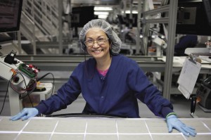
“There are close inspections along every step of the way to make sure everything is in working order, but the last bit of testing is the most crucial,” Santarris says. “We produce many panels per day, and we don’t want to go through that process only to find that there’s an imperfection in any of the panels we ship. Our business depends on our technological reliability, so we bring our workers back on to the line to make sure there are no flaws.”
Once the workers inspect and clean the panels, they are shrink-wrapped and prepared for shipping.
“We’ve made great strides in the process of building and creating solar panels, and we’re proud of what we’ve accomplished in the past three years,” Santarris says of the plant that started producing solar panels in 2008. “We are always looking to improve our processes, but we’ve done well so far. We’re looking forward to continued success long into the future.”


Tell Us What You Think!